This microscopic X-ray animation shows one of the key technologies allowing advanced computer functionality to fit within the smartphone in your pocket: ‘microvias’ are laser drilled holes a small fraction of a millimetre in diameter. A typical high-density interconnect printed circuit board might possess thousands of microvias, which serve to connect multiple functional layers.
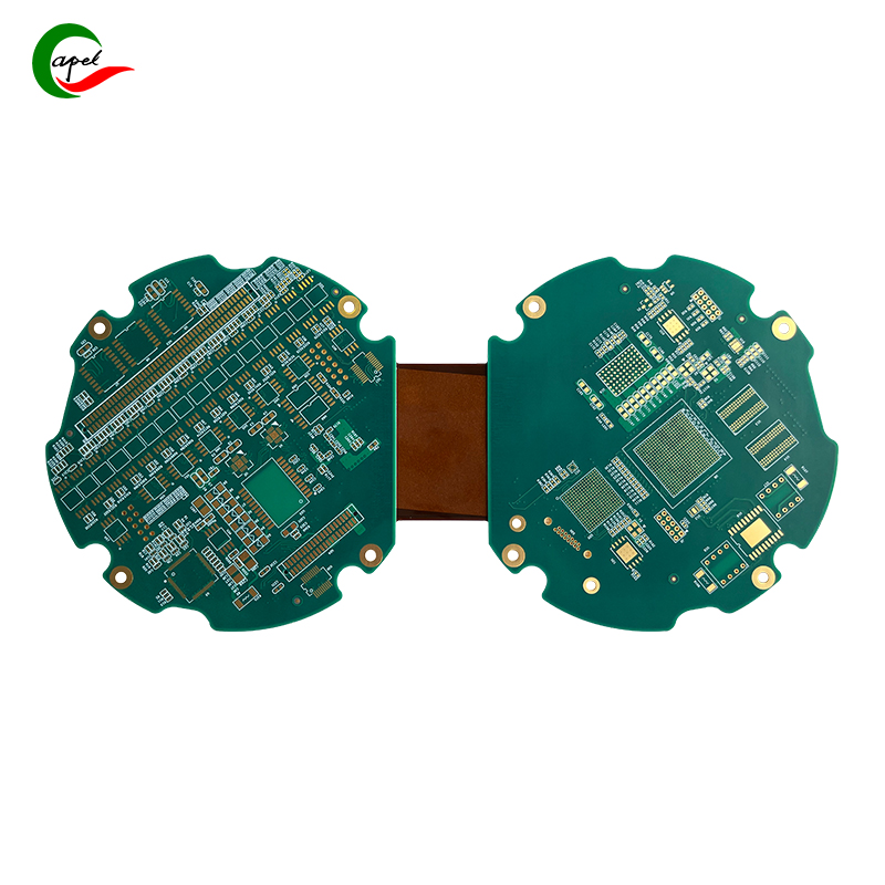
Microvias have enabled increased density and functionality for high density interconnect (HDI) printed circuit boards (PCBs) across a wide range of sectors, but they are subject to lingering reliability issues that has raised industry-wide concern. Now an ESA-led consortium has achieved the first qualification of HDI PCBs for space missions, representing a major step forward in quality control. Making Circuit Boards
ESA materials engineer Stan Heltzel, running the project, explains: ”Microprocessors and other electrical, electronic and electro-mechanical (EEE) components are how we embed intelligence into our space missions – along with non-space electronics – but they do not function in isolation. Instead they need to be interconnected and safeguarded against harsh external environments by being assembled together on PCBs.
“The high number of component input/outputs of modern chips, their small pitch and high signal speeds drive the need for short, dense and complex routing technologies in the PCB assembly – which is what we term HDI technologies.”
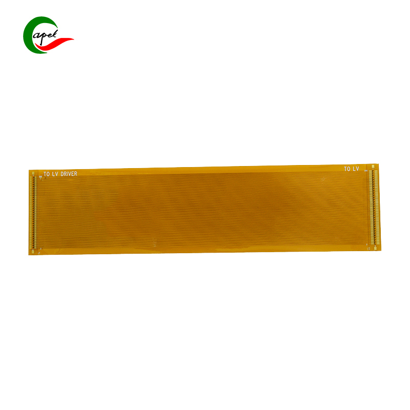
Demand for ever higher density interconnects means that PCB designers have reacted like architects in urban centres, and built upwards, by placing multiple copper layers within a PCB’s insulator material. These layers are connected together using microvias, which are first drilled, then cleaned using ‘wet chemistry’ and finally plated with copper to form an electrical link.
The problem? These microvias suffer from what the PCB industry calls ‘the hidden reliability threat’ – a major focus of current R&D. Microvia connections might seem healthy during lab testing, but elevated temperatures can cause the plated copper to pull away from the internal surface. Later, when inspected, the microvia link will have self-healed once the temperature has gone down again.
Stan adds: “This is a problem for the entire PCB industry but it is a particularly acute challenge for space, firstly because temperature extremes are commonplace, but also as our need for reliability is absolute.”
Specific HDI PCB qualification was, so far, not available as per the generic PCB guidelines of the European Cooperation for Space Standardization, ECSS – the common European rulebook for undertaking space missions. Instead, case-by-case project qualification is required for individual designs and batches, which is a significant hurdle in space projects.
But now PCB manufacturer ACB in Dendermonde, Belgium, has received ESA qualification for HDI PCBs, as the successful outcome of a recent General Support Technology Programme contract led for ESA by Belgian research institute IMEC, with Thales Alenia Space Belgium as end user.
Stan notes: “The road to achieve this was full of technical challenges as this advanced PCB technology is complex to manufacture and the failure modes are notoriously difficult to screen. Success involves reviewing the entire manufacturing process, involving dozens of process steps and hundreds of process parameters to be carefully audited. Improved testing was also part of the process, including making use of a ‘daisy chain’ of multiple microvias linked together to monitor their resistance during the hot phase of thermal cycling.
“This is an important achievement because European PCB manufacturers are relatively small in number, and must continue to innovate to enhance their competitiveness in global markets. The space industry definitely needs greater European PCB manufacturing, because building a close relationship with manufacturers is the best way to ensure the optimal quality control our missions need.”
Five papers have already been written from the consortium’s results, one of which received the best international paper award in the world’s most prominent conference IPC APEX EXPO 2020, as well as an honourable mention in 2022. And recently, the global electronics industry association IPC raised a European working group to further investigate microvia reliability, led by ESA and IMEC.
Meanwhile GSTP is undertaking similar HDI PCB qualification projects with manufacturers in France and Italy.
Pcb Board Maker You have already liked this page, you can only like it once!